
The Diode Current equation is obtained from the switching characteristics of devices, where the diode acts as a switch.
Diode as a Switch
When the diode is in forward bias, it conducts; when it is in reverse bias, it blocks. This can be used as an electronic switch.
1. When it is conducting, it acts as an ON switch.
2. When it is non-conducting, it acts as an OFF switch.
3. Let Vr represent the diode’s barrier potential or cut in voltage, Rf its forward resistance, and Rr its reverse resistance.
4. It is forward-biased if the applied voltage is Vi>Vr. Its models are V>Vr and V<Vr, and it functions as a closed switch.
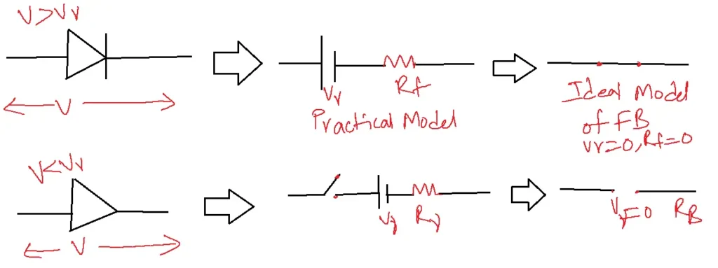
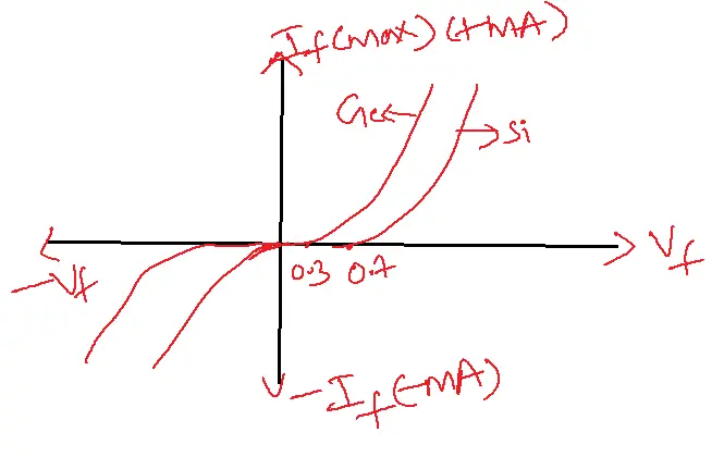
Table of Contents
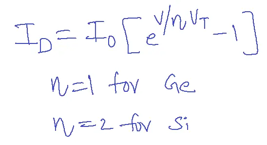
The current diode equation is given by
Io=Reverse Saturation Current
V = Applied Voltage
VT=Thermal Voltage (26mV) (KT/q)
The diode current equation, also known as the Shockley diode equation, is:
I = IS (e^(VD/VT) – 1)
Where:
– I, the diode current
– IS is the reverse saturation current (a constant)
– VD is the voltage across the diode
– VT is the thermal voltage (approximately equal to 25.85 mV at room temperature)
– e is the base of the natural logarithm (approximately equal to 2.718)
This equation describes the relationship between the voltage across a diode and the current flowing through it. It is a fundamental concept in understanding the behavior of diodes and is widely used in electronic circuit design and analysis.
Note:
– The equation assumes an ideal diode, with no series resistance or other non-idealities.
– The reverse saturation current (Io) is typically small, on the order of nano amperes or smaller.
– The thermal voltage (VT) depends on temperature, increasing with temperature.
The diode current equation can be simplified into three regions:
1. Reverse bias (VD < 0): I ≈ -IS
2. Forward bias (VD > 0): I ≈ IS * e^(VD/VT)
3. Breakdown region (VD < -VBR): I ≈ -IBR (where VBR is the breakdown voltage and IBR is the breakdown current)
Piece Wise Linear Characteristics of Diode
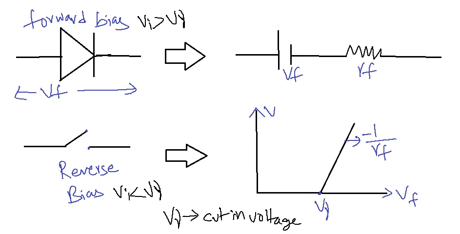
In large Signal analysis or engineering solutions, the diode is replaced by piece-wise representation.
The piecewise representation of the semi-conductor diode Vf – forward voltage is shown in the above figure.
rf is a forward resistance
Diode Switching Times
When a diode is switched from forward bias to reverse bias or vice versa it takes a finite time to reach the steady state value. This behavior of a diode is called the switching characteristics of a diode.
Naturally, whether the diode is forward-biased or reverse-biased, we would expect the conduction to proceed quickly, but this is not the case. A certain time elapses before the current in another mode can be reached.
Forward Recovery Time
Forward recovery time is the interval needed for the diode current to reverse and reach a steady state value when the diode runs in reverse bias and a forward bias is applied. It is represented with tfr[few nano seconds].
It does not create any problems with switching operations.
Reverse Recovery Time
Reverse recovery time is needed for the diode current to reverse and reach a steady state value when the diode is in conduction mode [FB] and the reverse bias voltage is applied. Practically it is several 100 ms. Hence it is required to consider thoroughly high-speed switching characteristics, represented by trr.
The diode’s operating frequency sets a limit on the overall switching time.
fmax = 1/10trr
Minority Charge Carrier Density Distribution function concerning distance x from the junction
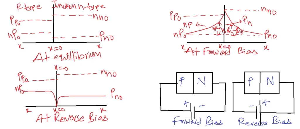
When forward biased, the majority charge carriers in the n-side and p-side cross the junction and they become minority charge carriers on the other side and the density function from the junction decreases exponentially by recombination with majority charge carriers.
When reverse-biased voltage is applied the density of minority carriers is shown by the solid line marked as pn and np. Away from the junction, the minority carrier density remains unaltered. However, these carriers pass the intersection quickly as they get closer to it, which causes the density of minority carriers to almost disappear.
Applications
The diode current equation has numerous applications:
1. Diode Circuit Design: Understanding diode behavior for rectifiers, clippers, and clamper circuits.
2. Solar Cells: Modeling and optimizing solar cell performance.
3. Semiconductor Devices: Analyzing and designing bipolar junction transistors (BJTs), thyristors, and other semiconductor devices.
4. Power Electronics: Designing and optimizing power conversion circuits, such as rectifiers, inverters, and switching power supplies.
5. Electronic Devices: Modeling and understanding the behavior of electronic devices, like LEDs, photodiodes, and transistors.
6. Integrated Circuit Design: Designing and optimizing integrated circuits, including analog and digital circuits.
7. Optoelectronics: Examining and creating optoelectronic devices, such as optical receivers and laser diodes.
8. Computer Simulation: Simulating diode behavior in circuit simulators, like SPICE.
9. Electrical Engineering: Understanding and analyzing diode behavior in various engineering applications.
10. Research and Development: Advancing diode technology and exploring new applications.
FAQs
1. What is the diode current equation?
- The diode current equation also known as the Shockley diode equation, describes the relationship between the current flowing through a diode and the voltage applied across it.
- It’s a fundamental equation in electronics, especially in pulse and digital circuits where diodes are commonly used for switching and rectification.
2. How is the diode current equation used in pulse and digital circuits?
The diode current equation helps:
- Predict diode behavior: It allows engineers to predict how much current will flow through a diode for a given voltage, which is crucial for designing circuits with specific operating points and switching characteristics.
- Analyze diode circuits: It’s used to analyze the behavior of diode circuits, including rectifiers, clippers, and clampers, under different input conditions.
- Design digital logic gates: The equation helps design and understand the operation of diode-based logic gates, foundational elements in digital circuits.
3. What are the limitations of the ideal diode equation?
The ideal diode equation assumes a perfect diode with zero resistance in the forward bias and infinite resistance in the reverse bias. However, real diodes deviate from this ideal behavior.
- Forward voltage drop: Real diodes have a small but non-zero voltage drop (typically around 0.7V for silicon diodes) even in forward bias.
- Reverse leakage current: Although reverse biased, a negligible amount of current, known as leakage current, flows through the diode.
4. How does temperature affect the diode current equation?
Temperature significantly impacts the diode current equation.
- Increased forward current: As temperature increases, the forward current through the diode increases for a given voltage.
- Increased reverse leakage current: The reverse leakage current also increases with temperature.
5. What is the role of the diode current equation in switching circuits?
In switching circuits, diodes are used to control the flow of current. The diode current equation is vital for:
- Calculating switching times: Understanding the time it takes for a diode to turn on or off is critical for designing high-speed digital circuits.
- Analyzing switching losses: This equation is crucial for estimating power losses during switching, a key factor in power efficiency.